
多路输出开关电源的设计
多路输出开关电源的设计(外文翻译,论文13000字)
摘要:各种精密的电子产品和实验仪器的普及,使得人们对电源提出了更高的要求。本文描述了一种低成本、高效率、安全便携的宽输入小功率多输出开关电源电路的设计方法及其应用。该系统使用UC3842芯片为控制核心,分析确定了反激式的主功率拓扑。电网滤波电路、输入输出整流/滤波电路、功率变换电路、控制电路和输出电压反馈电路构成了系统的主体。高频变压器与光耦使得输入输出的电气隔离。开关芯片,功率MOS管,TL431和光耦组成了反馈回路。4路输出中包括了主路和辅路,其中主路通过电压、电流反馈环调节开关芯片的PWM输出脉宽。整个系统实现了多路输出开关电源的稳定输出及较好的纹波抑制。
关键词:多路输出;反馈;反激式;隔离;开关电源
Multi-output switching power supply
Abstract:With the popularity of electronic products and various kinds of precision instruments, the requirements for power supply are also increasingly higher. This paper describes a kind of low cost, high efficiency, safety and portability of wide input design methods of low power multi output switching power supply circuit and its application. The system uses UC3842 chip as the control core, analyzed the main power flyback topology. EMI filter circuit, the input / output rectifier filter circuit, power conversion circuit, PWM control circuit and the output voltage feedback circuit system. High frequency transformer and opto electrical isolation between the input and output. Switch chip, the power of the MOS, TL431 and the composition of the optocoupler feedback loop. The 4 way output includes the main circuit and the auxiliary circuit, wherein, the main circuit is adjusted by the voltage and the current feedback loop to adjust the PWM output pulse width of the switch chip. The whole system realizes the output of multiple output switching power supply.
Key words:multiple output; feedback; flyback; isolation; switching power supply
设计的主要内容和技术指标
1)主电路能达到要求的多路输出;
2)能达到良好的控制效果,稳定的输出;
3)确定合理的拓扑结构和控制方式;
4)驱动电路和保护电路;
5)滤波电路相应的分析和变压器的设计;
6)相关电子元器件的选型(理论分析、设计计算、测试及数据处理、器件选型等);
7)主要技术指标:
电源输入: 50Hz,85~265V宽范围交流
电源输出:直流±5V,+15V,+7.5V
对应额定电流:1.0A,0.5A,2.5A
输出纹波: ≤±1%的输出电压
标准输入电压:交流电220V,50Hz。
工作温度:-25℃~80℃
输出电压准确度:≤5%
效率:≥80%。

目 录
1引言 1
1.1设计背景及研究意义 1
1.2本课题的国内外的研究现状 1
1.3 设计的主要内容和技术指标 2
1.4线性电源与开关电源 2
1.5开关电源的典型结构 3
1.6开关电源基本工作原理 3 [资料来源:Doc163.com]
2主电路设计 4
2.1多输出开关电源系统构造方案 4
2.2 拓扑结构 6
2.2.1几种基本的拓扑结构 6
2.2.2拓扑结构方案选择与论证 8
2.3输入过电压保护电路 9
2.4 EMI滤波电路 9
2.5整流/滤波电路 10
2.5.1整流结构 10
2.5.2整流滤波电路工作原理 11
2.5.3输入整流管参数选择 12
2.6无源吸收电路 13
2.7变压器选择及参数计算 13
2.7.1变压器磁芯的选择 13
2.7.2变压器匝数的确定 14
2.7.3变压器绕组线径的选择 14
2.8主要器件选择及功能介绍 15
2.8.1 TL431 15
2.8.2 PC817 15
2.8.3场效应管MOSFET 16
2.8.4高频变压器 16
3控制电路设计 16
[来源:http://Doc163.com]
3.1 控制模式选择 16
3.2 UC3842控制芯片 16
3.2.1 UC3842控制芯片简介 16
3.2.2 UC3842控制芯片特点 17
3.3 控制电路结构与工作原理 17
3.3.1控制过程 17
3.3.2稳压控制电路 18
3.4 过流保护原理 19
3.5 过压保护原理 19
3.6 开关管保护电路 19
4测试分析 19
4.1测试设备介绍 19
4.2测试结果及说明 20
4.2.1输出能力和精度测试 20
4.2.2纹波测试 20
4.2.3输出效率测试 21
4.2.4系统联调 22
5总结与展望 23
5.1设计总结 23
5.2开关电源发展展望 24
参考文献: 25
致 谢 26
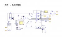
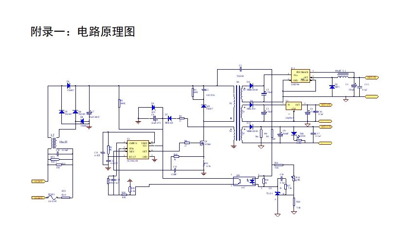
附录一:电路原理图 27 [版权所有:http://DOC163.com]
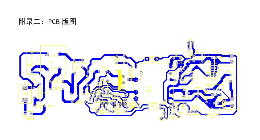
附录二:PCB版图 27
附录三:元器件清单 27 [资料来源:http://doc163.com]