
半导体激光器驱动电源的设计

半导体激光器驱动电源的设计(任务书,开题报告,论文说明书12000字)
摘 要
本论文主要阐述了半导体激光器(LD)驱动电源硬件和软件的设计开发。在LD原理和特点的研究基础上,设计了LD驱动电源的方案,实现了输出恒定电流,脉冲电流上升沿无过冲的功能。LD驱动电源采用基于运算放大器的压控恒流源电路,对电流进行控制,使用电流测量芯片实时检测电流大小,利用模拟开关切换触发模式。该电源的控制芯片采用赛普拉斯公司的CY8C3545LTI-163片上系统,该芯片集成了很多数字模块和模拟模块,使软件设计更加灵活。软件方面主要对通信模块、外触发检测模块、过流过压保护模块和电流缓启动模块这四方面进行设计和开发。通过对LD驱动电源的实际测试,该电源符合LD的使用要求。
关键词: LD 压控恒流源 电流缓启动 过流过压保护
Design of power supply for laser diode
Abstract
This paper mainly expounds the design and development of hardware and software for the laser diode (LD) driving power. Based on the research of the LD principle and characteristics, the LD drive power supply scheme was designed to achieve a constant output current and no overshoot at the rising edge of the pulse current. The LD driving power source uses a voltage-controlled constant current source circuit based on an operational amplifier to control the current. The current measuring chip is used to detect the current in real time and the analog switch is used to switch the trigger mode. The control chip of the power supply adopts Cypress's CY8C3545LTI-163 system-on-chip. The chip integrates many digital modules and analog modules, making the software design more flexible. The software mainly designs and develops four aspects: communication module, external trigger detection module, over-current and over-voltage protection module, and current slow-start module. Through the actual test of the LD drive power, the power supply meets the requirements of the LD.
Key Words: LD; Voltage controlled constant current source; Current slow start; Over-current over-voltage protection
[资料来源:http://Doc163.com]
目录
摘 要 I
Abstract II
目录 III
第一章 引言 1
1.1 选题背景 1
1.2 LD驱动电源研究现状 1
1.3 LD驱动电源发展趋势 2
第二章 方案设计 3
2.1 LD驱动电路设计 4
2.2 触发切换电路设计 5
2.3 通信及控制单元设计 5
第三章 硬件设计及开发 6
[资料来源:http://doc163.com]
3.1 压控恒流源电路 6
3.2 外触发隔离电路 8
3.3 触发模式切换电路 8
3.4 DA模块 9
3.5 外部供电保护电路 10
3.6 电流检测电路 11
3.7 通信模块 12
3.8 LD保护电路 13
3.9 控制芯片CY8C3245LTI-163 14
3.10 芯片供电电路 15
第四章 软件设计与开发 17
4.1 软件方案设计 17
4.2 外触发检测 17
4.3 状态监测 19
4.4 RS422通信 20
4.5 电流缓启动 23
第五章 测试与调试 25
5.1 调试平台搭建 25
5.2 模块测试 25
5.3 调试结果 26
第六章 总结与展望 30
参考文献 31
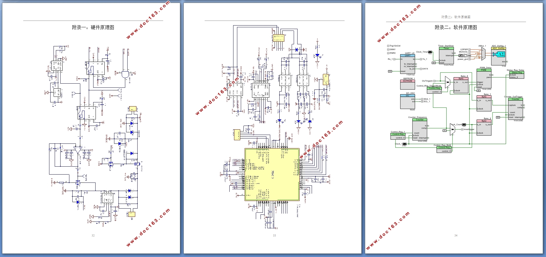
附录一:硬件原理图 32
[来源:http://Doc163.com]
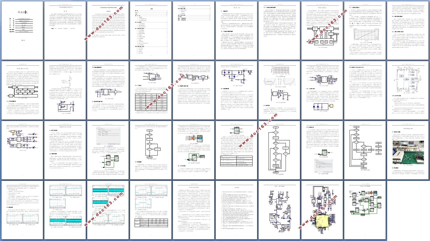
附录二:软件原理图 33 [来源:http://www.doc163.com]