
基于FPGA的数据采集器设计

基于FPGA的数据采集器设计(任务书,开题报告,外文翻译,论文14500字)
摘 要
随着数字技术的不断发展,对数据采集设备的要求也越来越高:一方面,要求其有比较灵活的接口和较高的数据传输速率;另一方面,在采集数据时要高效、准确且能对数据做出快速而又准确的响应。并能及时地对接收到的数据进行分析和处理。本文设计和实现了基于FPGA系统的数据采集器。
该系统使用FPGA作为系统控制核心单元,其优点是时钟频率高,内部延时小,FPGA可以在同一个时钟周期内进行多个操作,所以速度比较快,其次FPGA体积方面有很大的优势,体较小,管脚多。在FPGA内部实现了逻辑设计和嵌入式CPU NIOS软核的嵌入。通过对ADC0809电压采集芯片的控制来采集多路电压,并在FPGA内部实现和NIOS软核的通信。在NIOS中接收来自ADC0809将模拟电压信号转换为数字信号的转换完成标志,并在NIOS内部将数字数据转换为电压值。采集的速度是100us一次。将电压值通过串口输出给上位机PC;在PC上使用上位机软件可以实时观测电压数值,并且通过可调电阻改变输入的电压值的方式来实时在PC上观测电压的变化。
关键词:FPGA NIOS ADC0809 多路电压采集
FPGA-Based Data Acquisition Device
[来源:http://www.doc163.com]
Abstract
With the continuous development of digital technology, the requirement of the data acquisition devices are higher increasingly. On the one hand, it requires a relatively flexible interface and high data transfer rates; on the other hand, it requires efficient and accurate data collection and can make quick and accurate response when collecting data. At the same time, the devices should analysis and process the received data in time.
The system uses FPGA as the core of the system control unit, the advantage of the system is a high clock frequency and a small internal delay, FPGA can perform multiple operations in a single clock cycle, so the speed is fast. Secondly, there is a great advantage in the bulk of FPGA, it is small and the number of the pin is large. In the FPGA, logic design and embedding CPU NIOS soft core are realized. By controlling ADC0809 voltage collecting chip, multiple voltage can be collecting, and realize the communication with NIOS soft-core in FPGA. NIOS receives the flag of completion from ADC0809 that the analog voltage signal is already converted to digital signals, and convert digital data into a voltage value in the internal NIOS. The speed of collecting is 100us at a time. The voltage output to the host computer via the serial PC, voltage value can be observed in real time using PC software on the PC. At the same ,the change of the voltage can be observed on PC by the way changing input voltage using via an adjustable resistor. [资料来源:www.doc163.com]
Keywords : FPGA ;NIOS ;ADC0809 ;multiple voltage acquisition
目 录
摘要 I
ABSTRACT II
第一章 绪论 1
1.1 数据采集系统简介 1
1.2 数据采集系统的研究意义和应用 1
1.3 系统中主要研究内容和目的 2
1.4 论文结构 2
1.5 本章小结 3
第二章 系统工作原理及主要器件介绍 4
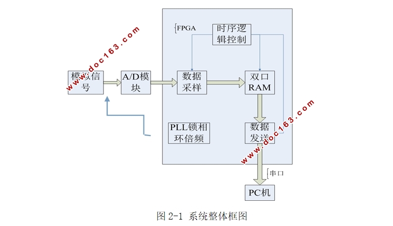
2.1系统的整体设计 4
2.2 FPGA芯片选型 4
2.3 ADC0809芯片 7
2.4 串口芯片MAX3232 10
2.5 本章小结 12
第三章 系统硬件电路设计 13
3.1硬件电路整体框图 13
3.2 FPGA核心电路 14
3.3 模数转换模块 16
3.4 分压模块 18
3.5 本章小结 19
第四章 系统软件设计 20
4.1 设计思路 20
4.2 实现代码 22
4.2.1 顶层介绍 22
4.2.2 各子模块设计 22
4.3 设计仿真 31
4.3.1 ADC模块仿真图 31
4.3.2数据采集和输出的仿真图 31
4.4 本章小结 32
第五章 测试及分析 33
5.1 硬件调试 33
5.2 调试结果 33
第六章 总结与展望 34
6.1 总结 34
6.2 展望 34
参考文献 35
致谢 37
[版权所有:http://DOC163.com]