
基于FPGA的数字锁相放大器的研究与设计
基于FPGA的数字锁相放大器的研究与设计(任务书,开题报告,论文18000字)
摘 要
微弱信号检测,是所有与实验测量密切相关的一门学科都避免不了的工作,无论是基础学科中的物理、化学、生物,还是高深的学科天文、地理、医学等等,都需要测量一些幅值很小的微弱信号,并且往往伴随着复杂的环境噪声。几十年来微弱信号检测技术蓬勃发展,技术逐渐成熟和完善,引起国内外各项科学领域的重视。
微弱信号检测的发展日新月异,各种技术、仪器层出不穷,本设计就是以其中的一种精密仪器为基础的,它就是锁相放大器(LIA)。这种仪器是利用相敏检测(PSD)技术来工作的,也就是所谓的相关检测技术,它是从信号的频率出发,通过判断频率是否与参考信号相同来进行检测,得到有用信号并消除噪声干扰,进而准确得出有用信号的幅值。最先出现的锁相放大器是模拟锁相放大器,但是模拟器件自身存在一些难以解决的缺陷,例如噪声较大、温度漂移、同步困难等。随着制造工艺进步,大规模集成电路开始出现,数字电路飞跃发展,这时候数字锁相放大器开始出现,它从源头上解决了模拟器件的诸多缺陷,并且还具备一些性能和经济上的优势,所以数字器件很快取代了模拟器件,成为了时代的主流。因此数字锁相放大器也很快被发明出来,并应用到各类科学研究领域中,发挥着巨大的作用。 [资料来源:www.doc163.com]
本文首先介绍了锁相放大器的研究背景与发展现状,提出主题;紧跟着介绍了锁相放大器的理论基础,也就是相关检测原理,然后详细解释相关解调算法并在此基础上提出双通道数字相关解调;然后是系统的硬件电路设计,包括信号通道的前置放大器、带通滤波器、A/D转换的电路设计,原始信号经过信号通道转换为数字信号进入FPGA系统;接下来是FPGA系统中的各个功能子模块的设计,包括参考信号的生成、数字锁相环、布斯乘法器、低通滤波器、求平方差等;最后将结果进行矢量运算求出幅值,通过LCD屏显示出来。
关键字:数字锁相放大器;数字锁相环;相关检测技术;Verilog HDL语言;FPGA
Abstract
Weak signal detection is a task that all disciplines closely related to experimental measurement can not avoid. Whether it is the physics, chemistry, biology, or advanced disciplines such as astronomy, geography, medicine, etc. A weak signal with a small value, and it is often accompanied by a complex environmental noise. For decades, the weak signal detection technology has developed vigorously and the technology has gradually matured and improved, drawing attention from various scientific fields at home and abroad. [资料来源:http://Doc163.com]
The development of weak signal detection is changing with each passing day. Various technologies and instruments emerge in an endless stream. This design is based on one of the precision instruments. It is a lock-in amplifier (LIA). This kind of instrument uses phase-sensitive detection (PSD) technology to work, which is the so-called correlation detection technology. It starts from the frequency of the signal, detects whether the frequency is the same as the reference signal, and obtains useful signals and eliminates noise. Interference, and then accurately get the useful signal amplitude. The first lock-in amplifier was an analog lock-in amplifier, but the analog device itself has some insurmountable drawbacks such as large noise, temperature drift, and synchronization difficulties. With the advancement of manufacturing technology, large-scale integrated circuits have begun to appear and digital circuits have developed rapidly. At this time, digital lock-in amplifiers began to appear. It solved many defects of analog devices from the source, and also had some performance and economic advantages. Therefore, digital devices quickly replaced analog devices and became the mainstream of the era. Therefore, digital lock-in amplifiers were quickly invented and applied to various scientific research fields and played a huge role. [来源:http://www.doc163.com]
This article first introduced the research background and development status of the lock-in amplifier, and proposed the theme; followed by the introduction of the theoretical basis of the lock-in amplifier, which is related to the detection principle, and then explain the relevant demodulation algorithm in detail and based on this proposed two-channel Digital correlation demodulation; then the system's hardware circuit design, including the signal path preamplifier, bandpass filter, A / D conversion circuit design, the original signal through the signal channel into a digital signal into the FPGA system; next is The design of each functional submodule in the FPGA system, including the generation of reference signals, digital phase-locked loops, Booth multipliers, low-pass filters, squared differences, etc.; finally, the results are subjected to vector operations to obtain the amplitudes through the LCD. The screen is displayed.
Key Words: Digital lock-in amplifier;Digital phase-locked loop;Correlation detection technology; Verilog HDL language;FPGA [资料来源:www.doc163.com]
[来源:http://Doc163.com]
目 录
摘 要 I
Abstract II
第1章 绪论 1
1.1 课题研究的背景 1
1.2 课题研究的目的与意义 1
1.3 锁相放大器的发展概况 2
1.4 课题研究的主要内容 2
第2章 数字锁相放大器的原理 4
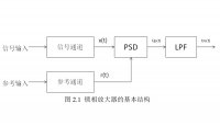
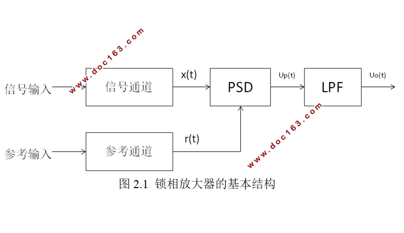
2.1 锁相放大器介绍 4
2.2 相关原理与相关函数 5
2.3 相关检测技术 5
2.4 信号的相关解调原理 7 [版权所有:http://DOC163.com]
2.4.1 模拟信号相关解调 7
2.4.2 数字相关解调算法 8
2.4.3 双通道数字相关解调 8
2.4.4 双通道相关解调器 9
2.5 基于FPGA的数字锁相放大器的总体设计 10
第3章 系统硬件设计 11
3.1 数字锁相放大器的总体硬件设计 11
3.2 前置放大电路设计 11
3.3 滤波电路设计 15
3.4 A/D转换电路设计 16
3.5 LCD接口电路设计 17
3.6 外围硬件电路设计 19
第4章 FPGA内部逻辑设计 21
4.1 FPGA技术简介 21
4.2 FPGA 内部功能模块结构 21
4.3 TLC549 A/D转换控制器的设计 22
4.4 FPGA 参考信号设计原理 24
4.4.1 鉴相器模块(DISCR) 25
4.4.2 数字环路滤波器(K模可逆计数器)模块 25
4.4.3 数控振荡器模块 26 [版权所有:http://DOC163.com]
4.5 相敏检波模块设计 28
4.5.1 90°数字移相电路设计 29
4.5.2 乘法器模块的设计 29
4.5.3 数字低通滤波器设计 30
4.6 幅值求解模块设计 31
4.7 锁相电路整体设计 32
5.1 原始信号的模拟 33
5.2 数字锁相放大器总体功能测试 33
总结 36
参考文献 37
附录 部分模块Verilog HDL代码 39
致 谢 43