
PDH通信一次群复接器在FPGA中的实现
PDH通信一次群复接器在FPGA中的实现(论文13000字)
摘要
数字复接技术是数字通信网的一项重要技术,能够将若干低速信号合并为一路高速信号,进而提高传输效率。应用可编程逻辑门阵列(FPGA)芯片实现PDH通信一次群复接器便于修改电路结构,增强设计灵活性,并且节约了系统资源。
本文首先介绍了EDA技术的发展情况及技术特点,然后对数字复接的原理以及方法进行了说明。采用自顶向下的建模思路,设计并详细的说明了复接器的模块组成,并在altera-modelsim软件中进行各个模块的仿真,给出了各个模块的流程图以及仿真结果。最后进行了复接结果的仿真。本文设计的PDH通信一次群复接器的主要功能是将32路64Kb/s低速码流,通过同步、采集、最后由复接模块复接为1路速率为2.048Mb/s的高速码流。由仿真结果可以看出,结果与设计相符。
关键词:数字复接;准同步数字系列;FPGA;VerilogHDL
Abstract
Digital multiplexing and demultiplexing,an important technique in the network of commu-nication,can improve the transmission effciency in the way of multiplexing several low speed data flows into a high speed one. In addition to better designflexibility and save system reso-urce, digital MULDEX system based on the FPGAalsomake the problem of modifying struc-ture of circuit easier. [来源:http://Doc163.com]
This paper first introduces the development of EDA technology and its technical characteristics.Then explain the principle and method of digital multiplexing .Using top-down modeling ideas,The module composition of the multiplexer is designed and explained in detail.The simulationof each module iscarried out in Altera-modelsim software, and give the flow chart and simulation results of each module ,Finally, the simulation of the multiplexing results is carried out.The main function of PDH communication one-time group multiplexer designed in this paper is to set the 32-way 64Kb/s low-speed code stream,By synchronizing, collecting, and finally connecting the Multiplexing module to a high-speed code stream with a 1-way rate of 2.048Mb/s.As can be seen from the simulation results, the results are consistent with the design.
Key words:Digital multiplexing;Plesiochronous DigitalHierarchy;FPGA;VerilogHDL
[资料来源:https://www.doc163.com]
目录
第1章 绪论 1
1.1 复接技术研究现状 1
第2章 EDA技术概述 2
2.1 EDA技术及其发展 2
2.1.1 EDA技术的发展历程 2
2.1.2 EDA技术的的独特之处 3
2.2 硬件描述语言 3
2.2.1 Verilog HDL 3
2.2.2 基于Verilog HDL的自顶向下设计方法 4 [资料来源:www.doc163.com]
2.3 EDA技术的发展趋势 5
第3章 复接原理及技术 6
3.1 复接技术的发展 6
3.2 复接器的组成 8
3.3 复接的方法 8
3.4 复接方式 9
第4章 PDH通信一次群复接器的FPGA建模与设计 11
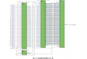
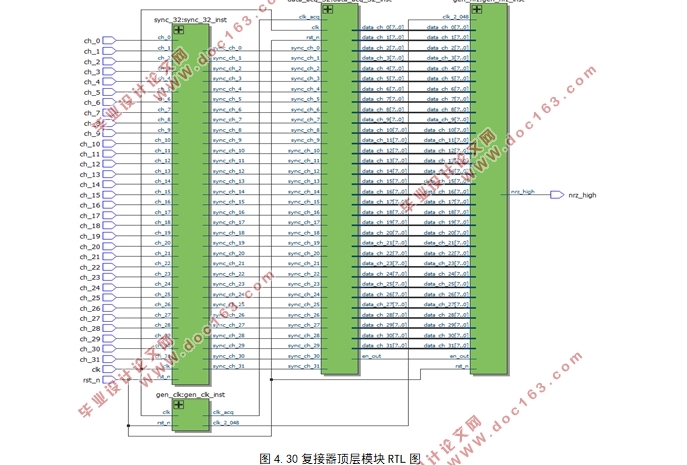
4.1 PDH通信一次群复接器的模块组成 11
4.1.1 时钟源生成模块 12
4.1.2 同步模块 16
4.1.3 采样模块 18
4.1.4 高速码生成模块 21
4.2 PDH通信一次群复接器验证与仿真 27
4.2.1 仿真结果 28
结语 34
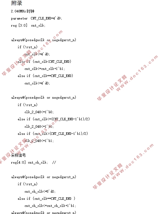
附录 35
参考文献 42
[资料来源:https://www.doc163.com]